How to Read a Schematic: A Beginner's Guide to Circuit Diagrams
Learn to read electronic schematics: a symbol chart, reference designators, component values like 4k7 and 104, a worked LED circuit, and how a diagram maps onto a real circuit board.
Written by Kerem Başbuğ · Last updated September 16, 2026 · How we rank
7 min read
Affiliate disclosure: As an Amazon Associate we earn from qualifying purchases. We may earn a commission when you buy through links on this page — at no extra cost to you. Read our affiliate disclosure for details.
A schematic is the map of a circuit. It does not show what the board looks like — it shows what connects to what. Once you can read one, a kit stops being a mysterious bag of parts and becomes something you understand, can troubleshoot, and can eventually modify. It is the most valuable non-soldering skill in electronics.
Schematic vs layout
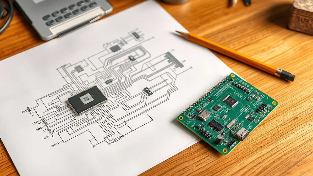
First, an important distinction. A schematic is the logical diagram: it shows the components and their electrical connections, arranged for clarity, not for physical position. The PCB layout is the physical realisation — the actual board, with copper traces where the schematic shows wires. The same schematic can be laid out as a board in countless ways. Learn the schematic and you understand the circuit regardless of how it is physically built.
Common schematic symbols
A handful of symbols cover most beginner circuits:
| Component | What the symbol looks like | Designator |
|---|---|---|
| Resistor | Zig-zag line (US) or a small rectangle (IEC) | R |
| Potentiometer | Resistor with an arrow pointing into it | R or VR |
| Capacitor | Two parallel lines | C |
| Electrolytic capacitor | One flat and one curved plate, or a + sign | C |
| Diode | Triangle pointing at a bar — current flows toward the bar | D |
| LED | Diode symbol with two small arrows pointing away | D or LED |
| NPN / PNP transistor | Circle with three leads; the arrow on the emitter points out (NPN) or in (PNP) | Q |
| Integrated circuit | Box with numbered pins | U or IC |
| Inductor | A row of loops or bumps | L |
| Switch | A break in the line with a lever | SW or S |
| Push button | Two contacts bridged by a small T-shaped plunger | SW |
| Fuse | Rectangle with a line through it, or an S-shaped line | F |
| Crystal | Rectangle between two plates | Y or X |
| Speaker / buzzer | Small box with a cone, or a semicircle | LS or BZ |
| Connector / header | Small circles or boxes with pin numbers | J or P |
| Battery | Long and short parallel lines (long is +) | BT |
| Ground | Downward set of shrinking lines, or a triangle | — |
You do not need to memorise them all at once; you will recognise them quickly through use. Kits like the Elenco project kit often print the schematic alongside the build, which is a great way to learn by matching symbol to part.
Power and ground
Most schematics do not draw a battery wired to every part. Instead they use power labels:
- VCC, VDD, +5V, 3V3 — the positive supply. “3V3” means 3.3 V; the letter replaces the decimal point.
- GND — ground, the 0 V reference everything returns to, drawn as a stack of lines or a triangle.
- VEE / VSS — negative or 0 V supply rails on some chips.
Every symbol with the same label is the same net. A chip with a “VCC” pin and a capacitor with a “VCC” label elsewhere on the sheet are wired together, even with no line between them.
Following the connections
The heart of reading a schematic is following the nets — the connections:
- A line is a wire. Every point joined by lines is electrically the same node.
- A dot at a junction means connected. Four lines meeting with a dot are all joined.
- Lines crossing without a dot are not connected — they simply pass over each other on the page.
- Labels join things too. A wire labelled “VCC” or “LED_EN” connects to every other net with the same name, even across different sheets.
Reading a schematic is mostly a matter of tracing these nets: start at the power source, follow the current through components, and see where each net goes. Signals usually flow left to right, with power at the top and ground at the bottom.
Reference designators
Every component has a label — R1, C3, D2, U1 — called a reference designator. The letter tells you the type and the number tells parts of the same type apart. The same designator appears on the PCB silkscreen, which is how you match a part in the schematic to its spot on the board when you solder — and how you find the right component when troubleshooting.
Reading component values
Values are written next to the designator, often in a compact shorthand:
| Written as | Means |
|---|---|
| 220R or 220Ω | 220 ohms |
| 4k7 | 4.7 kΩ (the “k” replaces the decimal point) |
| 1M | 1 MΩ |
| 100n | 100 nF (0.1 µF) |
| 104 (on a ceramic capacitor) | 10 + four zeros pF = 100 nF |
| 10µ or 10uF, 25V | 10 µF electrolytic, rated 25 V — observe the + side |
| 3V3 | 3.3 V |
Letters-as-decimal-points exist because a printed dot is easy to lose; “4k7” can never be misread as 47k. On the parts themselves, resistor values are printed as colored bands — our resistor color code calculator decodes them.
A worked example: a simple LED circuit
Picture the smallest useful schematic: a +5V label, a resistor R1 220R, an LED D1, and a GND symbol, all joined in a line.
- Start at power. The +5V label is the positive supply.
- Follow the net to R1. Current passes through the 220 Ω resistor, which limits it.
- Continue to D1. The triangle points toward the bar, so this LED is the right way round when its anode (triangle side) faces R1 and its cathode (bar side) faces ground. On the part itself, the cathode is usually the shorter leg and the flat edge of the LED.
- End at GND. The circuit is complete.
With a typical red LED dropping about 2 V, the resistor carries the remaining 3 V, so the current is roughly 3 V ÷ 220 Ω ≈ 13 mA — comfortably bright and safe. The LED resistor calculator does this sum for any supply and LED. If the LED does not light when you build it, this map tells you exactly what to check: power at the resistor, the LED’s orientation, and a solid ground joint.
How to read a circuit board
Sometimes you have a board and no schematic. You can still read a lot from it:
- Silkscreen designators (R1, C2, U1) tell you what each part is, matching the schematic if you find one later.
- Polarity marks — a + sign, a shaded half-circle, or a flat edge on the outline — show which way diodes, LEDs and electrolytic capacitors go.
- Pin 1 markers — a dot, notch, square pad or triangle — show chip orientation.
- Traces are the wires. Follow them from pad to pad to see what joins what; a multimeter’s continuity mode confirms connections hidden on inner layers.
- Wide traces and large copper areas usually carry power or ground.
Common mistakes when reading schematics
- Assuming crossing lines connect. Only a junction dot joins them.
- Missing a net label and thinking a pin is unconnected.
- Confusing the diode direction. The bar is the cathode — it faces ground in a normal LED circuit.
- Mixing up the IC pin order. Schematic symbols arrange pins for readability, not by physical position; always check the datasheet pinout.
- Ignoring the value’s units. 100n and 100µ differ by a factor of a thousand.
Why it makes you a better builder
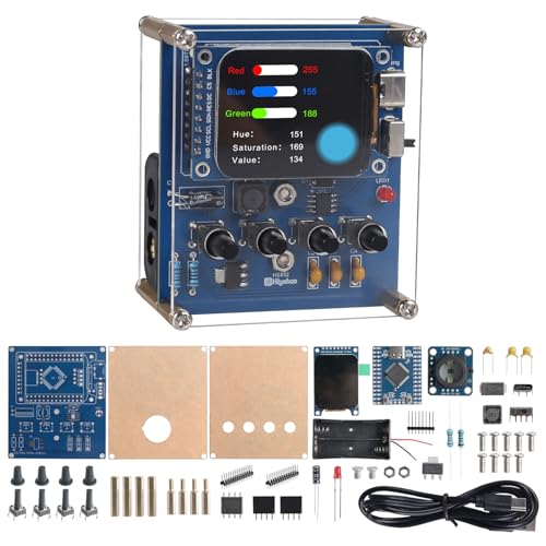
When a kit does not work, a schematic is your debugging tool. You can trace whether power reaches a chip, check that an LED is the right way round, or confirm a switch is wired correctly — none of which is possible if the board is just a pattern of parts to you. Understanding the circuit also turns a kit like the colour-sensor board or the Arduino-compatible Testudo into a platform you can actually experiment with.
Start by reading the schematic that comes with your next kit while you build it, symbol by symbol. Pair that understanding with clean joints from our beginner soldering guide and you are no longer just assembling electronics — you are learning them.
Recommended kits from this guide

amomii
amomii Testudo Soldering Practice Kit
Three real gadgets, guided tutorials, and an Arduino-compatible brain.
We earn a commission, at no extra cost to you.
BANRIA
BANRIA Color Recognition Soldering Kit
A real colour sensor and TFT screen — practice that teaches electronics.
We earn a commission, at no extra cost to you.

Elenco
Elenco Practical Soldering Project Kit (SP-1A)
The classic learn-to-solder kit that builds a working device.
We earn a commission, at no extra cost to you.